All you need to know about your products!

| 3DNews Vendor Reference English Resource - All you need to know about your products! |
||||||
 |
||||||
|
|
||||||
Debut of AMD AM2: the long-awaited DDR2 on AMD Athlon X2Date: 23/05/2006Author: , Dmitry Sofronov
This day can be called a reference point of the new epoch of AMD's processor architecture. It's just today when AMD has announced a start of delivery of dual-core AMD Athlon 64 FX-62 and AMD Athlon 64 X2 5000+ processors compatible to the new AMD Socket AM2, which support the AMD Virtualization technology and non-buffered DDR2 memory. Of course, along with the top-end processors there has been announced a whole line of new chips AMD Athlon 64 X2, AMD Athlon 64 and AMD Sempron compatible to the Socket AM2. Indeed, the long-awaited implementation of support for the DDR2 memory by AMD chips is undoubtedly an eminent event, although the processor core this time hasn't undergone any radical changes. The single- and dual-core processors for the new Socket AM2 that have been announced today offer a new controller with support for the DDR2. Along with that, for the first time there has been implemented support for a number of new technologies, with the operation of already known functions optimized, and several other architectural innovations introduced. However, in terms of evolution it doesn't reflect anything more than the new core stepping - Revision F. Consolidating the real architectural innovations announced today, we can count the following four points:
The key event underlying the transition to anew version of AMD processors for desktop PCs with the new 940-pin AN2 socket is the implementation of support for the DDR2 memory. Since the memory controller is integrated into the processor, the major complication of the stage is not the emergence of new memory chips (fortunately, the DDR2 has already gained wide occurrence and even gone down in price), and even not the emergence of some special chipset versions for the new platform (although, the need for good chipsets has always been there). The major point is how well AMD has managed to implement this integrated controller with support for the DDR2, To start with, let's sort out all the information on new chipsets available to date and then move on to running the tests. 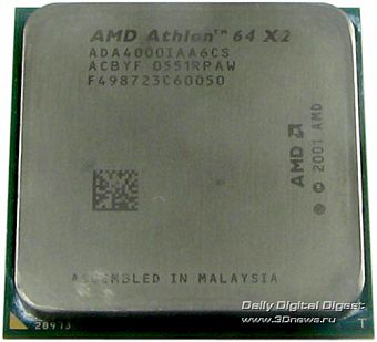 ArchitectureThe new AM2 processors by AMD are 940-pin K8 chips for desktop systems with support for the 128-bit DDR2 aimed at the new Socket AM2. From this point onwards, retail shops will be receiving more and more AM2 versions of AMD chips for all the market sectors - Athlon 64, Athlon 64 X2, and Sempron. These chips are consolidated by the DDR2 version of the Revision F processor core, although each sector has its own code name.
Although that is some deviation from the topic, I must point out that with the mass emergence of DDR2 versions of cheap AMD Sempron chips expected already this summer the epoch of wide use of the DDR1 memory can be regarded as quickly coming to a demise. In this regard, the quickness is of course a relative thing, and there are no plans yet to close down production of Socket 939 processors, but anyway that should be a distinct sign for reasonable buyers... The new revision F with the former 90-nm process technology, support for the fast memory up to DDR2-800, declared Pacifica technology, economical power saving have called foe some internal re-design. On the photo below, where dual-core chips of revisions E and F are compared, the easiest to see is the increased pad between L2 caches. 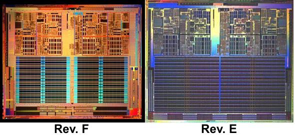 Windsor VS Toledo Actually, the drawing reproduces the scale in merely a schematic view. In fact, the area of the new core of Rev. F has been increased relative to version Rev. E by approximately 13% - up to 220 sq.mm (from 194 sq. mm). Therefore, the size of 1 MB L2 caches has been increased accordingly by 18%, so has the size of 1 MB L2 caches – from 106 sq. mm in Rev. E (in the first steppings - 115 sq. mm) to 126 sq. mm in processors of Rev. F. At the same time time, the areas of positioning SRAM L2 cache memory has gone down. While the 1 MB L2 cache size in Rev. E takes 41.4 sq. mm (therefore, 82.8 sq.mm for the dual-core structure), this indicator in new processors of Rev. F has gone down to 38.7 sq. mm (77.4 mm in the dual-core version). The number of transistors that constitutes each chip has gone up. While in today's dual-core K8 processors there are 233 mln transistors, then in chips of Rev. F there are 243 mln, that is, by approximately 4% greater. There is a complete analogy with single-core processors: 120 mln transistors in the single-core K8 chip have been replaced with 129 mln transistors in the processor of Rev. F, where the increase is even greater - i.e.by 7.5%. Increase in the core area with the reduction of cache area and the same process technology for the manufacture of processors of Rev. F suggest some reasoning. Indeed, AMD K8 chips of steppings Rev. D and Rev. E have been produced following the same 90-nm process technology PD-SOI (Partially Depleted Silicon-on-Insulator), with a 9-layer copper metallization. Therefore, the area of SRAM cells in the cache has gone down, the number of transistors has gone up, so has the total area of the chip. Of course, all can be attributed to the new DDR2 memory controller (indeed, support for DDR2-800 in exchange of DDR-400 called for substantial remake of signal lines) and support for the Pacifica technology, but it seems to me something will be "ticking" in these processors for the time being. For instance, integrated but not yet declared support for the Presidio technology (an analog to Intel's LaGrande). For now it is still unknown what to do with the virtualization – AMD Pacifica, like the 64-bit computing implemented in the architecture, may also wait until the emergence of the new generation of Microsoft Vista operating systems. Indeed, judging by the latest publications online, a substantial redesign of the core (the core, not the memory controller) is expected with the release of further steppings - Revision G and Revision H. In the case of Rev. G, at least a substantial redesign of the branch processing module is expected, and in Rev. H - even a new generation of the FPU (Floating Point Unit). 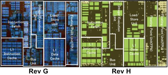 Schematic sketch of potential cores of Rev. G and Rev. H In this article, it doesn't make any sense to dwell on the details of the next generation of AMD64 architectures; anyway, I would note the newly born revision of the core hasn't undergone any substantial redesign which directly affects the performance. In other words, the performance boost, albeit expected, is possible only through the rise in clock speeds and implementation efficiency of the new memory controller. However, there is one more substantial change implemented in new AM2 processors of revision F, because chip versions with varying power consumption have been declared. Now, AMD will produce economical processors for desktop PCs of the Energy Efficient Desktop Processor class. This category includes a number of new Socket AM2 chips AMD Athlon 64 X2, AMD Athlon 64 and AMD Sempron with support for AMD Cool‘n’Quiet and improved power consumption. The new economical chips will be grouped into two subclasses - one with TDP 65 W and one with TDP 35 W. Just imagine that now you can come across three versions of the chip with a very similar name in the retail shop - AMD Athlon 64 3500+ or 3800+ , one of them being "regular", with TDP 89 W, the other one - Energy Efficient, with TDP 65 W and finally the third version - Energy Efficient Small Form Factor Desktop Processor AMD Athlon 64 X2, with TDP 35 W. Processors AMD Athlon 64 3500+ and 3800+ will be represented in versions for Socket 939 and Socket AM2, the same is for the case with AMD Sempron 64 3000+, 3200+, 3400+, 3500+, and 3600+ processors. 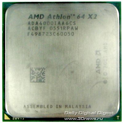 Let's introduce you to the participants of today's tests. Of course, the AMD Athlon 64 X2 4000+ processor is not a top-end chip in the new line of Socket AM2 processors and is unlikely to break records today. On the other hand, let's look closer at one of the potentially most popular chips – perhaps, it is to the better. The processor is marked as follows: AMD Athlon 64 X2 Let's sort out the OPN of this chip - ADA4000IAA6CS. The first three letters "ADA" which stand for the brand and make, are customary enough, like the four following digits which stand for the PR-rating of the processor. On the other hand, there is no character "I" in the current version of the document "AMD Athlon 64 Processor Power and Thermal Data Sheet". By analogy with the existing notation for this position, where "A" stands for the 754-pin OµPGA packaging, and "D" – the 939-pin OµPGA, we arrive at the conclusion that this time onwards the character "I" has been assigned to 940-pin chips for Socket AM2. The following two characters – "A" and "A" denote the core voltage and the chip package temperature, respectively. Foe both these cases, we find in the tables that "A" stands for "Variable". That's about all. The table that decodes the value of the following figure like L2 cache size ends with "5", which means 1 MB. This implies that "6" should stand for 2 MB (2 х 1MB). The last two characters stand for the chip's stepping. The official data ends with "CG" – Rev. E4, so "CS" is likely to meet some version of Rev. F.  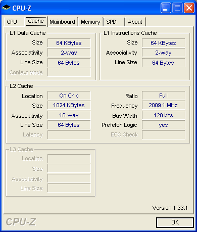 The data acquired with the CPU-Z utility confirms these figures and brings in additional definition on the core's supply voltage and the chip's stepping - Rev. F2. 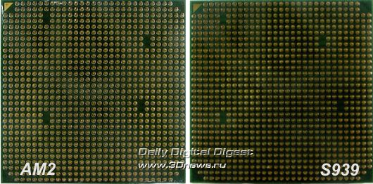 Examination of the exterior of a Socket AM2 processor and Socket AM2 as compared to Socket 939 shows that apart from adding one more pin the positioning of "caps" has been changed, so you won't be able to insert a 939-pin chip into Socket AM2. Some sort of a "fool-tolerance". I mean a fool not armed with a hammer. 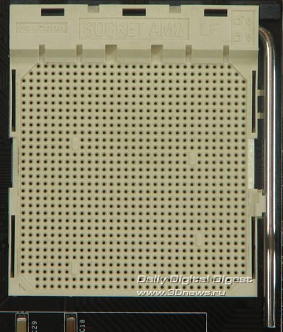 Along with that, of note is the changed fastening of cooling system in systems with Socket AM2. Instead of the customary numerous projections in Socket 754/940/939 systems, in Socket AM2 we find one symmetrically positioned projection to fasten a cooler on each side. 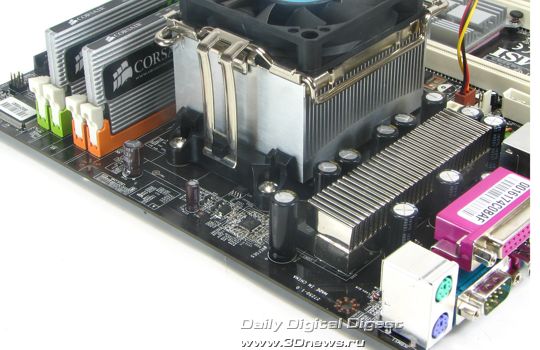 Among the participants of today's test is the MSI K9N SLI Platinum motherboard made in the ATX form factor aimed at operation with Socket AM2 processors AMD Athlon 64/X2/FX.  The motherboard is based on the NVIDIA nForce 570 SLI chipset, supports up to four DIMM DDR2-800 modules in the dual-channel mode (up to 8 GB altogether), is equipped with two PCI Express x8 slots (one of them offers support for PCI Express x16), two PCIe x1 slots, three PCI 2.3 slots, four SATA2 interfaces with support for RAID 0, 1, 0+1, and 7.1-channel HD Audio, Dual Gigabit LAN, ten USB 2.0 ports, etc. 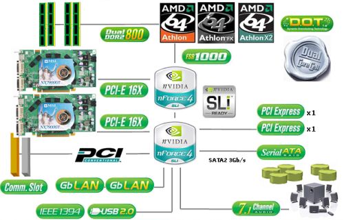 The board is also remarkable for its support of the Dual CoreCell technology with the overclocker feature D.O.T. Express and noiseless cooling of components - Silent Heatsink. On the whole, the new series of NVIDIA nForce 500 chipsets, whose start of deliveries is timed for the announcement of Socket AM2 chips, is made up of four modifications for each market sector where nForce4 SLI X16, nForce4 SLI, nForce4 Ultra, and nForce4 used to dominate.
A few brief notes on the specifications of the chipsets. The Link Boost technology implemented in nForce 590 SLI means that in case of using the nForce 590 SLI chipset with the GeForce 7900 GTX graphics the peak performance of the interface goes up by 25% - from 8 GB/s to 10 GB/s. 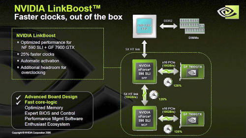 We already wrote about the so-called "SLI Ready" of EPP memory (Enhanced Performance Profiles) in our news and publications. Such memory has already been announced by Corsair Memory, so have to wait till the kits appear in our test labs for running tests. 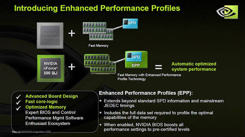 The TCP/IP Offload is familiar to us from versions of chipsets for server applications. It is now available in most chipsets of nForce 500 series, with its operating principle depicted on the slide below. 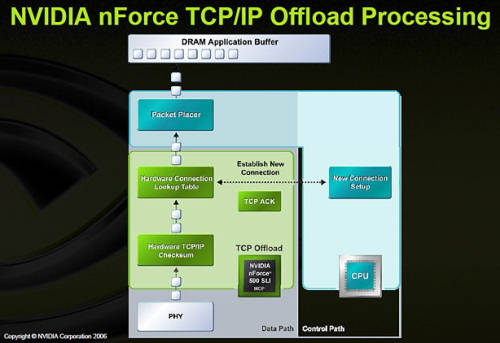 As regards support for the Teaming technology, its idea is about joining two Ethernet MAC levels which are present in chipsets of the new series, to double the bandwidth of the channel. In other words, using two integrated 1Gbps LAN controllers, it is possible to get a unified LAN controller of performance up to 2 Gbps. 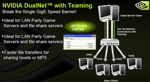 Finally, the FirstPacket feature that optimizes priorities of sending data bursts, including VoIP applications. 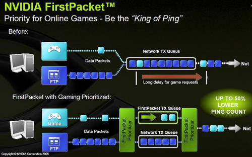 The key item of today's tests is a kit of two 240-pin CM2X1024-6400PRO memory modules of XMS2 6400 series made by Corsair Memory, of 1 GB capacity each, with the latency timings 5-5-5-12. In the end, we used the following components in the test bench: Motherboard MSI K9N SLI Platinum (NVIDIA nForce 570 SLI) 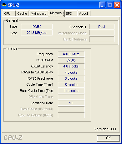 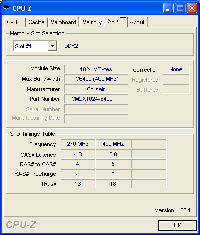 As a contender platform, we assembled a system on the following components: Motherboard MSI K8N Diamond Plus (NVIDIA nForce4 SLI x16) 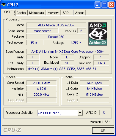 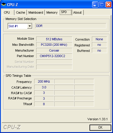 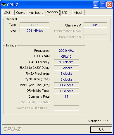 For the purpose of adequate comparison of platforms, we created similar test conditions which were attained as follows: the multiplier of Athlon 64 X2 4200+ is set to 10, that is, the resultant clock speed is set to the same value - 2000 MHz. Synthetic benchmarksAt the very start, we found out the following: since no modifications to the processor core which would affect the performance of new AM2 chips have been introduced, we should look for dependence of performance variation on the mode of memory controller operation. Since in the new AMD processors (like in "old" К8) all depends on the HyperTransport and there is no FSB at all, the memory controller integrated into the chip does not match any memory type starting with DDR2-400 and DDR2-533 up to DDR2-667, DDR2-800, and even DDR2-1066. That is why the major focus in our tests was made on selecting the most varied memory operation modes, i.e. we were after an in-depth investigation of variations to the system performance versus the memory frequency and latency timings. Of course, for curiosity we might have added results of tests for other AMD chips or other processor architecture into the comparison tables. But there was no sense in that, because found it more visual to approximate the difference in performance of Socket AM2 and Socket 939 systems to other reviews describing Socket 939 chips instead of depleting our results through bringing in fewer tests of the Socket AM2 system with various memory settings. On this page, we present the results of test in synthetic benchmarks. For convenience, we highlighted the DDR2 memory operation mode in yellow tints, and in green - for systems with DDR400. After the memory type, there go the memory latency timings at which we ran the tests. Let's start with Everest Ultimate ver. 2.80.534. 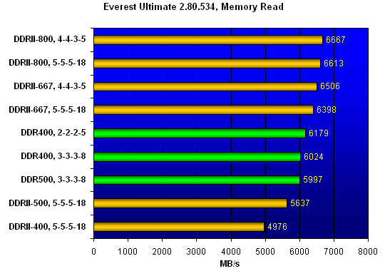 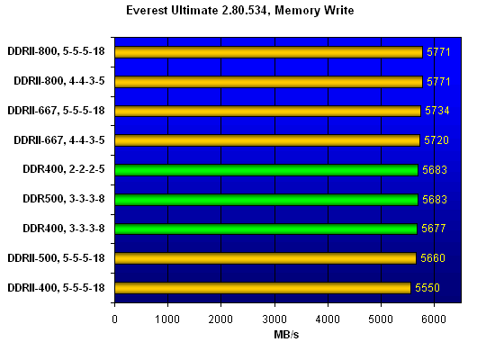 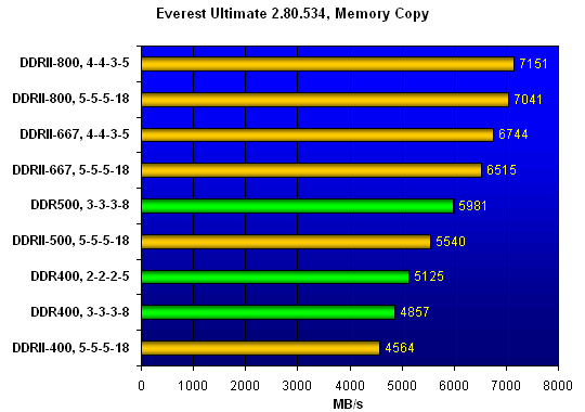 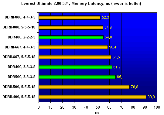 The very first results vividly prove the thesis that AMD processors with support for DDR2 memory would have had nothing to do in the epoch of DDR2-533 occurrence, let alone DDR2-400. As is seen in practice, the more or less impressive "gap" is seen just in a system with DDR2-800 that offers quite decent latency. Even DDR2-667 sometimes loses to the regular not overclocked DDR-400. Now let's see what PCMark'05 will show. 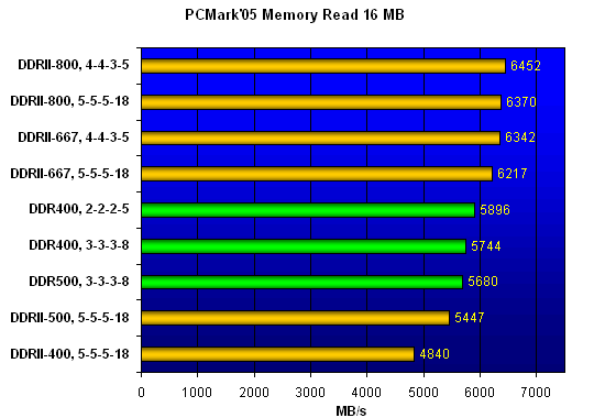 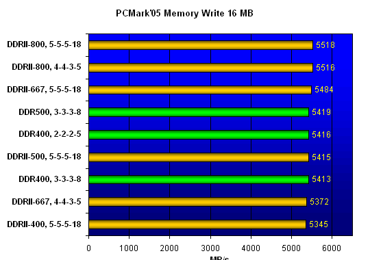 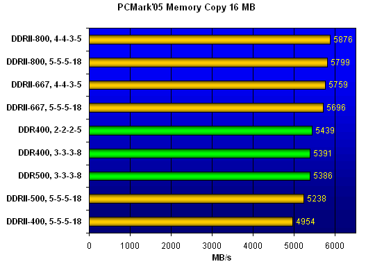 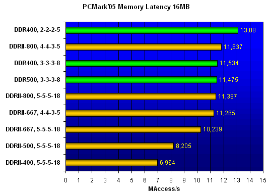 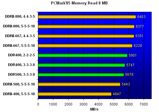 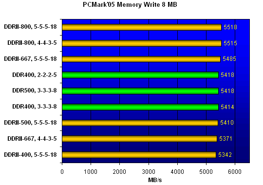 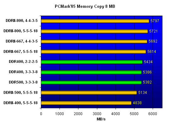 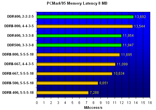 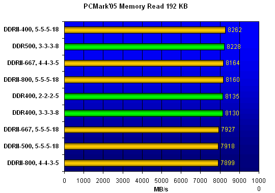 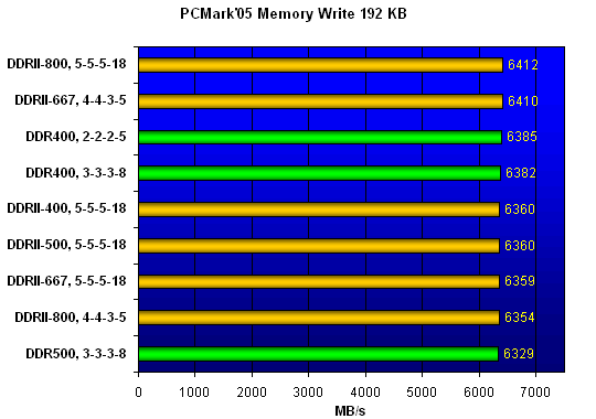 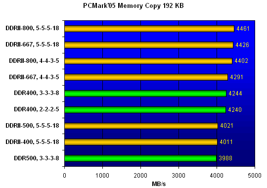 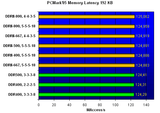 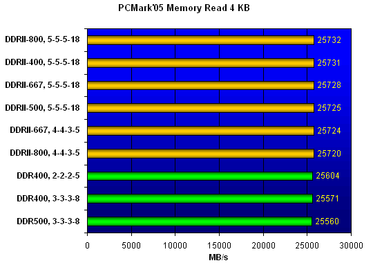 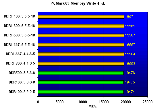 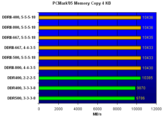 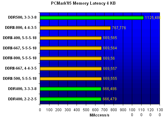 On the whole, the above stated is proved well enough by the results of tests run in PCMark'05. And this is the final verdict by PCMark'05: 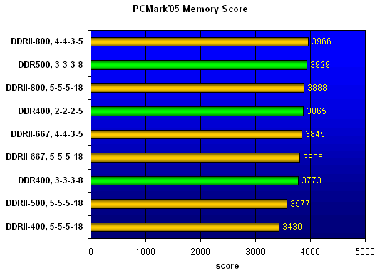 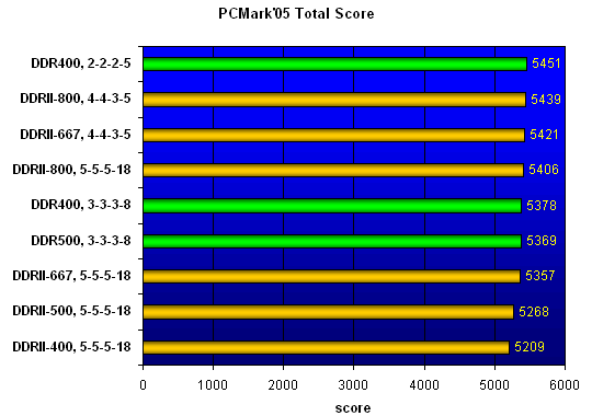 Summing up the results of testing the new system in synthetic benchmarks, we note that in general the latency and performance of DDR400 memory is in fact comparable to a system equipped with DDR2-667 4-4-3. That is, being guided by the test results, if I, say, were after replacing a system based on Socket 939 Athlon 64 X2 and DDR400 memory and if the retail didn't offer anything better than a combination of the same Athlon 64 X2 for Socket AM2 and DDR2-667 memory, then such a replacement would hardly be reasonable. Quite a different thing would be DDR2-800, but in any case the buyer should carefully examine the price tags for this memory before the purchase. We now will see how reasonable that will be when tested in real applications... Tests in real applicationsPrior to running tests in real applications, there is another key test - 3DMark 2005 Pro. 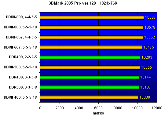 In this benchmark, the "reputation" of DDR2-667 looks much more firm, although we must admit that even the higher-end DDR2-800 system is no bargain either. There is some expected boost, which is a fact. But no more than that. Now let's see what the test system is worth of in real applications. 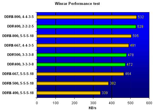 All the benefices are cut down at the roots because of the high memory latency. Whatever you do, at this test the DDR1 performs well enough, although losing the leadership. Now, a few typical and hard-edged gaming 3D tests. 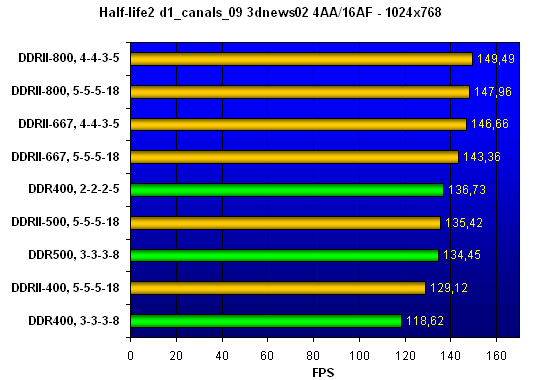 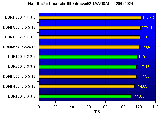 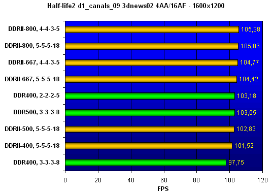 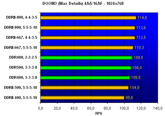 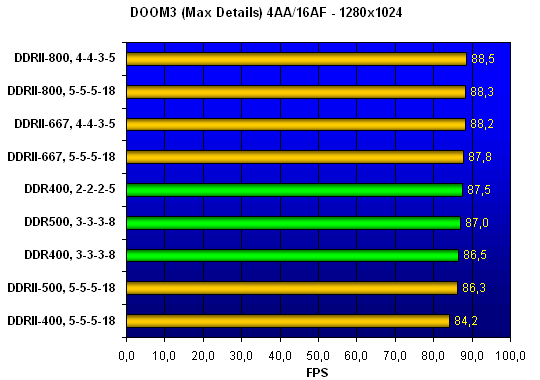 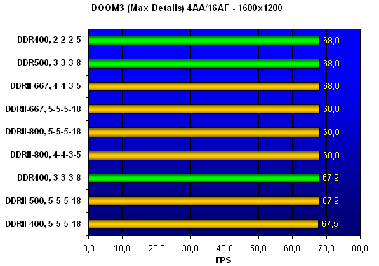 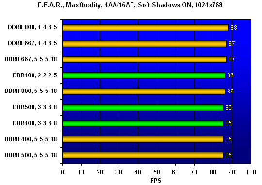 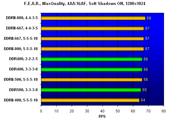 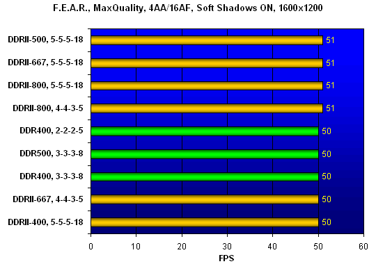 That is in fact all what was to be proved. Yes, in gaming applications the situation is the same - if you can't buy DDR2-800, you'd better wait a while. Even if it is used, the performance boost does not exceed the limits of measurement error. Final words and conclusionsWell, has the first DDR2 "pancake" by AMD proved lumpy? Despite the numerous "buts", this debut can't be called faulty. At least, because with the component base already available on sale you can get quite acceptable results, albeit not significant, but exceeding the capabilities of the previous generation. Another thing is whether it makes sense hurrying with purchasing a Socket AM2 system right now. The new processors of equal clock speed are normally a little bit more expensive than their Socket 939, and it is unlikely that their TDP reduced from 89 W to, say, 65W (the 35W versions are even more expensive) can be a strong incentive for that. But what about the prices for memory? It is of course up to you where and what to buy, but judging by the current prices, purchase of DDR2-800 modules will cost about one third more expensive than a similar DDR2-667 kit, and it will be about 10% cheaper to buy DDR400 with CL2. DDR2-533 will cost almost twice as cheap, but judging by the tests it will hardly be of use in combination with Socket AM2. Anyway, it does make sense to upgrade or, if possible, to migrate to a new platform already now. I won't dare to approximate the results of today's tests onto the higher-end models of the Socket AM2 line, but in any case it does make sense to plan a replacement of the platform simply because Socket AM2, to all appearances, seems to be with us for a relatively long time. At least, the next revision of the core - Rev. G, whose announcement is promised for December 2006 will be definitely manufactured for Socket AM2. Along with migration to the new 65-nm process technology, the new cores will have the computational modules improved with the cache further optimized, which will certainly improve the performance. It is also quite evident that now the number of new "overclocker-friendly" announcements and even regular DDR modules will come to null in the nearest time. Now they will be suitable for nothing more more than the VIA EDEN platform where high speeds have never been a must. On the whole, migration of the industry to DDR2 can be called as settled, albeit not complete. I think by the New Year eve this migration will be practically complete, and DDR1 with its price going up will unlikely be rescued by inexpensive Socket 939 Sempron processors. Finally, there is the answer to another interesting question. Did it really make sense for AMD to wait for the mass emergence of DDR2-800 in order to release a core with support for this memory type, or maybe Socket AM2 chips should have appeared earlier to leave the painful migration to a new processor socket behind by that time? Those who have glanced over this material may simply smile ironically when answering the question. Indeed, the delays did make sense for AMD. The other and quite pleasant side of this delay is the high readiness of the industry, especially motherboard manufacturers, for releasing products into the retail. All has long been verified and checked repeatedly, and all what was needed to wait for today's say-so from AMD... |
|
|||||