All you need to know about your products!

| 3DNews Vendor Reference English Resource - All you need to know about your products! |
||||||
 |
||||||
|
|
||||||
Gigabyte 780SLI-DS5 на NVIDIA nForce 780i SLIAuthor:Date: 18/01/2008
The release of Intel X38 has dramatically overturned the market of top-end motherboards. This product used to be the only one to offer support for the PCI Express v2.0, and the number of lanes was sufficient enough to arrange two full-featured PCI Express x16 slots. Although the expansion options of X38 are restricted by the functionality of the ICH9(R) bridge, this product is in demand on the market since it offers support for new processors manufactured following the 45-nm process technology. Moreover, Intel is speeding up this direction and preparing a new version - X48 for release, which implements support for the 400 MHz (1600 MHz QPB) bus. How will NVIDIA respond to the activities of Intel, its competitor? By and large, NVIDIA could do nothing at all: its top-end nForce 680i SLI chipset offers similar expansion options, and in terms of support for the PCI Express bus it offer a "conditional" superiority. We call it "conditional" because 680i SLI supports greater number of lanes and allows arranging three PCI Express x16 slots following the 16+16+8 formula. Certainly, 680i SLI does not support PCI Express v2.0 specifications, but currently this technology does not bring any performance gain. Nevertheless, support for the PCI Express v2.0 is a powerful marketing plus, and NVIDIA should have somehow responded to that. There are two more important points to note. Despite that Intel X38/X48 and nForce 680i SLI are both aimed at LGA775 processors, motherboards based on these chipsets are not competitors. The thing is that all the advantages of X38/X48 are revealed in only high-end systems which use two AMD video cards set to the Crossfire mode. The same situation is with nForce 680i SLI: a motherboard based on this chipset reveals its capabilities only if the SLI technology is used. The second important point is related to support for new 45-nm Yorkfield and Wolfdale processors. That is the major pain in the neck for NVIDIA: boards of the reference design had very serious issues operating these processors. And the chipset nForce 680i SLI itself is not to blame for that: the manufacturers who produced motherboards of their in-house PCB design did not come across these issues. Certainly, NVIDIA released patch to the BIOS, but that looks a half-measure because it cuts the performance down. After all, NVIDIA weighed all the pros and cons and released a new generation of nForce 7xx chipsets, which includes the two products: nForce 780i SLI and nForce 750i SLI. As the names suggest, they are aimed to replace nForce 680i SLI and nForce 650i SLI. Of the two novelties, we are more interested in nForce 780i SLI since we acquired one of the first boards built on this chipset - the Gigabyte 780SLI-DS5. Let's examine the nForce 780i SLI in more detail. On paper, all the above issues with nForce 680i SLI have been solved. In particular, motherboards of the reference design built on nForce 780i SLI will support 45-nm Yorkfield and Wolfdale processors (but for now only the 1333 MHz bus). The second improvement - nForce 780i SLI supports the PCI Express v2.0 bus, while the total number of bus lanes has gone up to 62 (!), of which 32 lanes conform to the v2.0 specifications. Such functionality was implemented in the following way: engineers at NVIDIA have added an additional chip - nForce 200 which provides support for 32 PCI Express v2.0 bus lanes. Schematically, this looks like that: 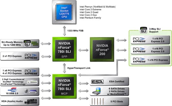 Therefore, engineers at NVIDIA have simply renamed 680i SLI SPP and 680i SLI MCP to 780i SLI SPP and 780i SLI MCP and, quite probably, the new chips offer a "higher" in which some minor improvements and fixes have been made, with some minor shortcomings eliminated. If our version proves right, this technical solution has the following substantial shortcoming: the 32 PCI-E v2.0 bus lanes from the nForce 200 bridge are linked to 16 PCI-E v1.0 lanes which were originally implemented in 680i SLI SPP. Therefore, we get the so-called "bottleneck" which in theory degrades the performance of PCI Express x16 v2.0 video cards. However, in practice the user may not notice this issue because the bandwidth of PCI-E v2.0 is not yet in demand and still won't be in demand for quite a long time. We are even confident that the performance of Triple-SLI will be about the same on 680i SLI and 780i SLI chipsets. Therefore, from the marketing perspective, the 780i SLI SPP chipset is a big leap forward. But its practical advantage is merely in a guaranteed support for 45-nm Yorkfield and Wolfdale processors. But in view of the fact that the date of release of Intel processors with the 400 MHz (1600 MHz QPB) bus, the lifespan of nForce 7xx SLI series chipsets will not be long. However, there aren't any technical limitations in the new chipsets for operation at this frequency, because as our overclocking experiments have shown, these chipsets are quite capable of running at 500 MHz as well. As regards the expansion options, they have not been improved: The south bridge 780i SLI MCP supports six SerialATA II links (levels RAID 0, 1, 0+1, 5), one ParallelATA link, ten USB 2.0 ports, HDA (Azalia), and two Gigabit network connections. At the same time, there is support for all NVIDIA's proprietary technologies like MediaSheild, FirstPacket, DualNet, etc. Gigabyte 780SLI-DS5 Specifications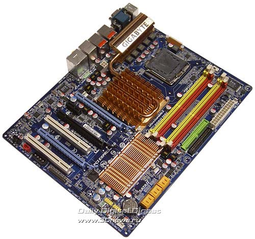
Layout and FeaturesThe first thing what catches the eye is the huge dimensions of ASUS Maximus Extreme. And that has not misled our eyes - it is an inch larger (269x305 mm): 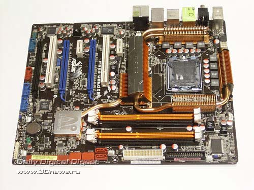 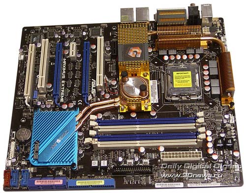 We are already used to massive cooling systems mounted on ASUS' top-end boards. And P5E3 Deluxe is no exception: radiators are around the CPU connector from all the sides. But cooling of the Maximus board is even more advanced: on the north bridge of the chipset, there is a water block combined with a really huge radiator. Therefore, even without a water-powered cooling system the temperature of the chipset stays within acceptable limits. By the way, this radiator uses a rectangular unit with a Republic of Gamers logo which is highlighted effectively. 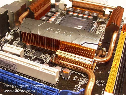 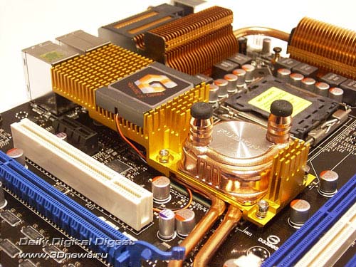 Each motherboard has four 240-pin DIMM slots each for DDR3 memory modules, with the overall supported memory capacity being 8 GB. 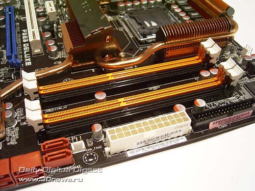 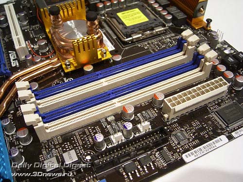 The configuration of the slots is identical for both the boards. These are three PCI Express x16 slots, two PCI Express x1, and two regular PCI slots. 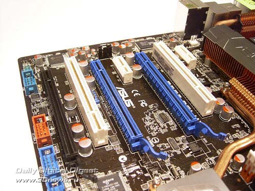 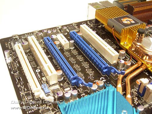 The PCI Express bus lanes are distributed as follows. If two video cards are installed, 16 lanes is allocated to each. If three video cards is installed, the lanes are distributed following the 16+16+4 scheme. Besides, the Maximus Extreme board offers the 16+8+8 configuration owing to the Crosslinx configuration. Both the motherboards use the ICH9R south bridge with a radiator. In the end, both the boards offer support for six SerialATA II ports located near the south bridge. 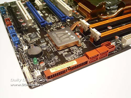 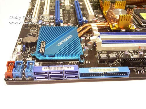 Besides, the boards use an additional ParallelATA/SerialATA JMB363 controller. 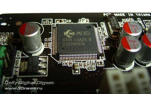 This chip supports one ParallelATA and two SerialATA II links (on both the boards, the SATA ports are brought over to the rear panel). Therefore, to each of the boards the user can plug in ten hard disks (eight SATA + two PATA). Then, the south bridge ICH9R supports 12 USB2.0 ports. They are implemented as per the following scheme: six integrated ports (on the rear panel) + 6 additional (plugged in with brackets; the board comes bundled with 1 plate for 2 ports). Besides, both boards support the Firewire. For that, there is an additional controller. On the ASUS P5E3 Deluxe board it is a FW3227 chip made by Agere, and on the ASUS Maximus Extreme - a VT6308P chip made by VIA. 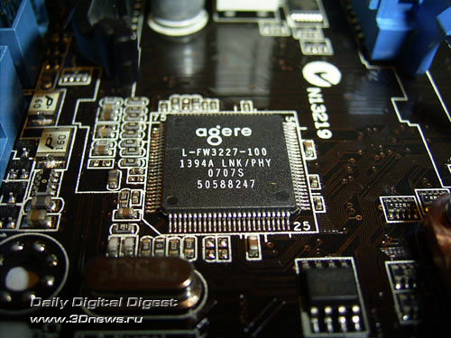 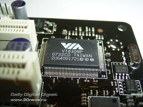 In the end, the motherboards support two ports each, with the layout being similar: one mounted on the rear panel, with the other ones connected with a bracket (available in the package bundle of both the boards). The motherboards implement the Intel High Definition Audio subsystem: ASUS P5E3 Deluxe uses an AD1988B chip, and ASUS Maximus Extreme - the same chip but installed on a separate board with a special screen protecting against induction. 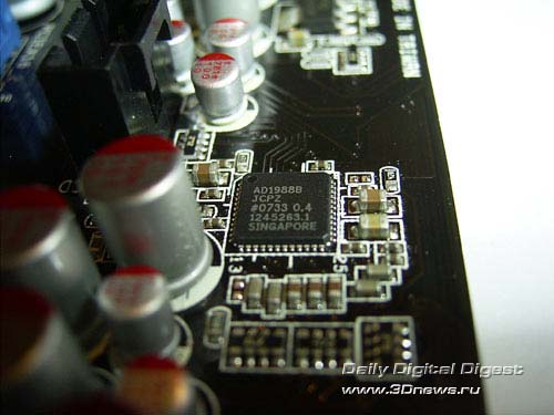 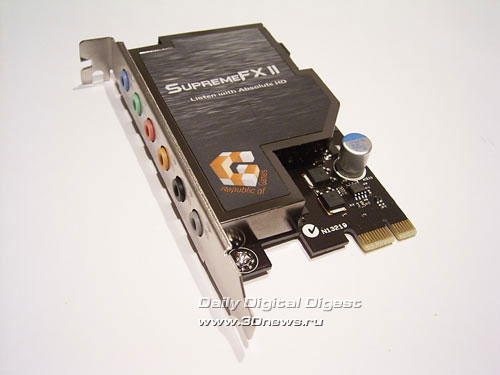 A few words on the network support: each of the boards uses two Gigabit LAN controllers. In particular, on ASUS P5E3 Deluxe these are Marvell 88E8056 (PCI Express x1) and Realtek 8110SC (PCI) chips, 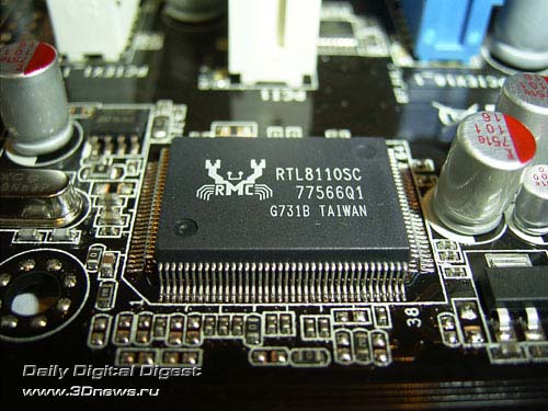 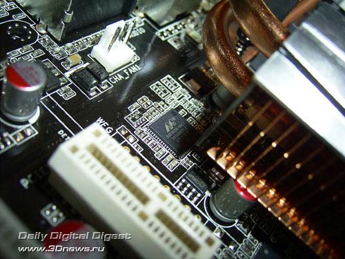 and on the ASUS Maximus Extreme - two Marvell 88E8056 (PCI Express x1) controllers. The board's rear panel is of the following configuration: 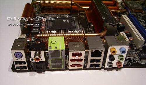 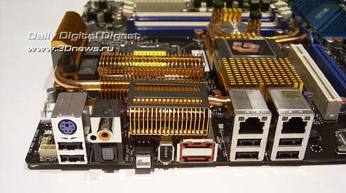 In terms of functionality, both the panels are similar: there is an optical and coaxial SP-DIF outputs, a Firewire port, a couple of SATAII ports, and six USB 2.0 ports. On the Maximus Extreme board, there is a button to clear the CMOS settings (works only at a certain position of the CLRTC_SW switch), a connector to plug in the LCD-Poster, and in the upper part there is one of the radiators. You can also notice a complete lack of LPT and COM ports. However, ASUS P5E3 Deluxe supports one serial port (COM) but implemented with a bracket (missing in the bundle). Here is a schematical drawing of the motherboards: 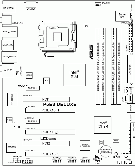 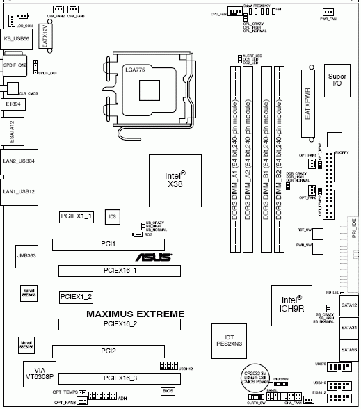 Among the special traits of the board, we note only the three buttons: Power, Reset, and ClrCMOS which are installed on the Maximus board and are meant to start up, reboot the system, and to clear the CMOS settings. The first two buttons are positioned near the DIMM slots: 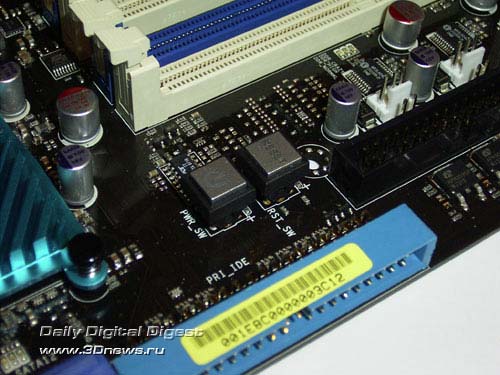 Now on to the BIOS settings. BIOSThe BIOS of both the boards is based on the AMI BIOS version, with its capacity being 16 Mbit. 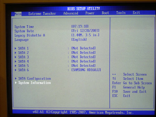 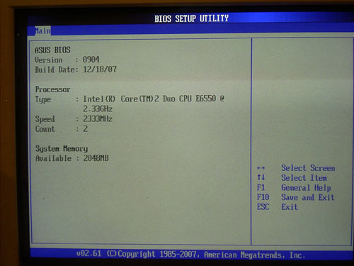 The section in charge of memory operation settings looks like this: 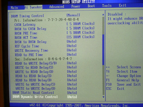 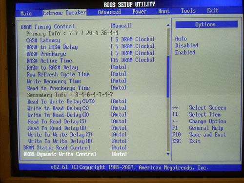 Additional adjustment to the memory can be performed with the "DRAM Static Read Control" and "DRAM Dynamic Write Control": 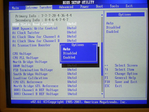 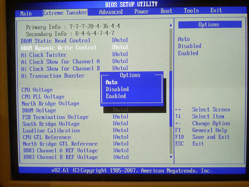 For that, there are the "DRAM Command Rate" and "Ai Transaction Booster" parameters: 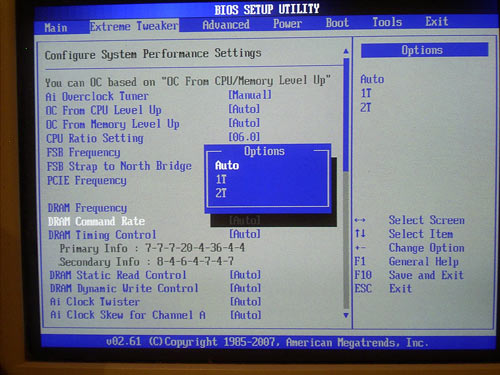 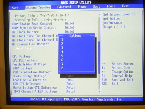 Another important parameter that affects the performance is setting the memory operating frequency. The set of available frequency multipliers coincides for both the boards: 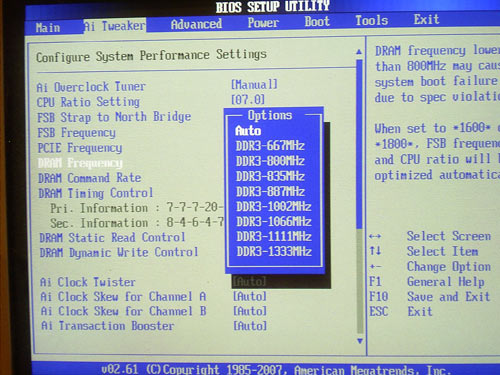 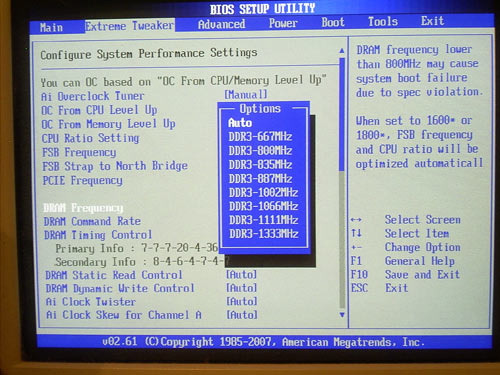 Now look at the system monitoring section. At that, P5E3 Deluxe lags well behind the Maximus Extreme model. 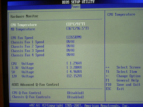 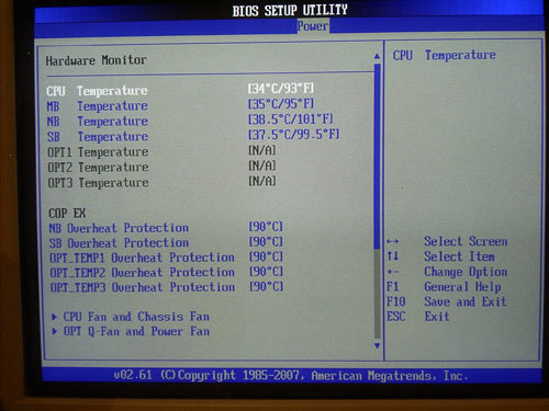 In particular, the Maximus model not only keeps track of the CPU and the system but indicates the temperature of the north and south bridges. Moreover, the board determines the temperature from three external thermal sensors (available in the bundle) and thus allows the user to monitor the cooling efficiency of the whole computer. 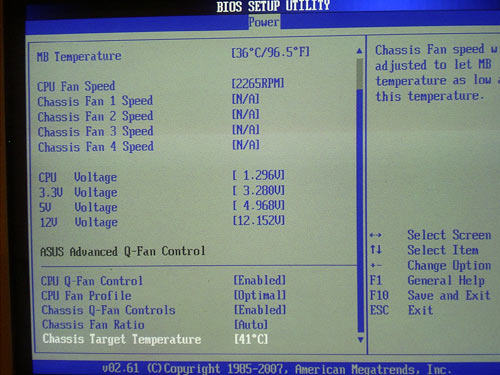 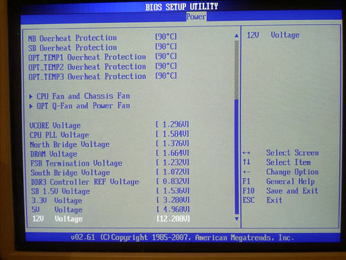 The thing is, the Maximus model offers independent adjustment of the Q-Fan feature for four (of eight) fans, with three can be "linked" to the temperature of the external thermal sensor. 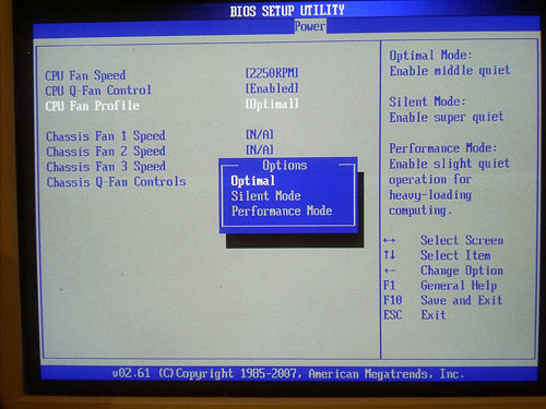 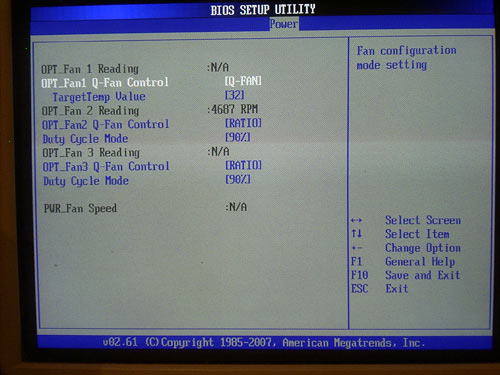 Both the motherboards are able retaining and loading BIOS settings as profiles. 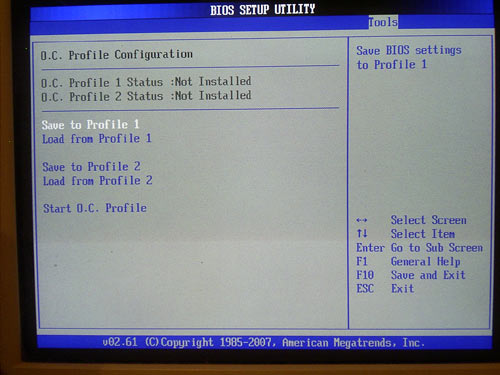 To update the BIOS, the ASUS board offers the integrated EZ Flash 2 utility: 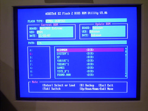 We also note the feature for displaying the BIOS settings in multiple languages, and a section to control the functions of Intel processors: 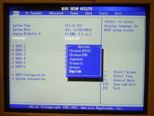 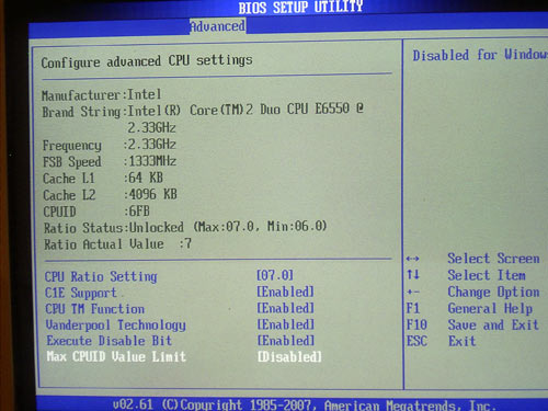 Overclocking and stabilityBefore we move on to Overclocking, let's look at the power converters. The PWM of ASUS P5K3 Deluxe uses a 8-phase scheme in which there are eleven 561 mkF and two 271 mkF capacitors. The PWM of the ASUS Maximus Extreme also offers a 8-phase scheme in which there are twelve 561 mkF capacitors. 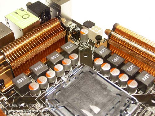 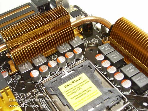 All the power components of the PWM on the boards are equipped with radiators, and on ASUS P5E3 Deluxe there is an additional radiator on the power converter of the memory modules. Besides, user of both the boards can raise the cooling efficiency through installation of additional fans (available in the package bundle). Now on to the overclocking features. They are gathered in the "Ai Tweaker" section. 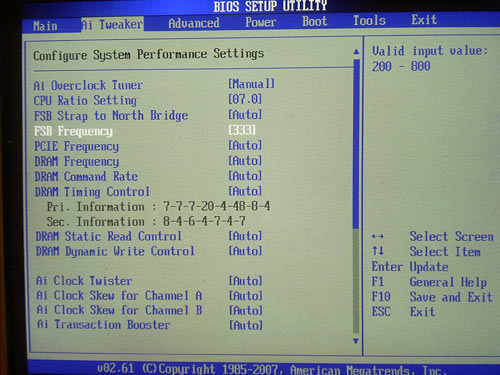
We note the following traits of the motherboards at overclocking. First, programmers at ASUS have added the feature for highlighting the parameters exceeding the range of safe overclocking (in their opinion) with different colors. Also, the ASUS boards lack the ASUS NOS (Non-Delay Overclocking System) technology which is implemented on almost all the previous models by this manufacturer. Instead, there is support for the X.M.P., CPU Level UP, and Memory Level UP (the latter two are only in the Maximus Extreme model). 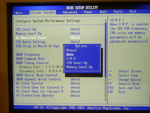 The X.M.P. technology means support for the Intel XMP (Extended Memory Profiles). This is some sort of an analog to the NVIDIA EPP (Enhanced Performance Profiles) technology whose idea is in the additional information written into the SPD of the memory modules, where guaranteed stable memory operation parameters are embedded. Each set includes information on the memory frequency, voltage, respective latency timings, and most importantly, the sub-timings. Therefore, overclocking with the X.M.P.e is performed based on the memory capabilities: the memory frequency is set to the maximum possible and then, with the available multipliers, the FSB (and thus the CPU clock speed) is set. The second feature - CPU Level UP - is somehow simpler and easier: the Maximus board offers a fixed set of FSB/MEM frequency values, and for better perception each set meets the specifications of an Intel processor. 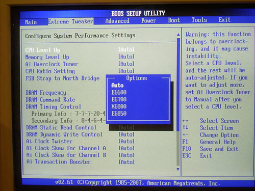 For details of using this feature in practice, read a review of ASUS Maximus Formula (DDR2). Here, we merely note that the "Memory Level UP" features operates in absolutely the same manner as the name suggests - it is memory that is overclocked. 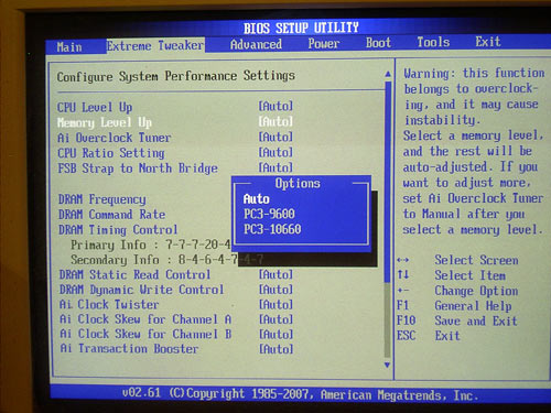 Despite the kindred BIOSes, the Maximus board is much superior at the adjustment convenience. The thing is, while setting voltages the P5E3 has no menu, which in our view is somehow inconvenient. Let's look at the practical results of overclocking which proved to be equally high. The maximum stable FSB speed in ASUS boards is 568 MHz, which is a record for our test lab.   We even re-tested the CPU E6550 and found out that it was capable of running stably at 3.92 GHz (versus the nominal 2.33 GHz)! The previous achievement was 3.85 GHz, and you can take a look at the performance of this CPU at this clock speed in this review. 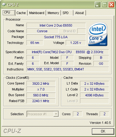 Performance testsWhile determining the starting FSB speed, it turned out that both the boards overstated it (the P5E3 Deluxe - by 1.3 MHz).  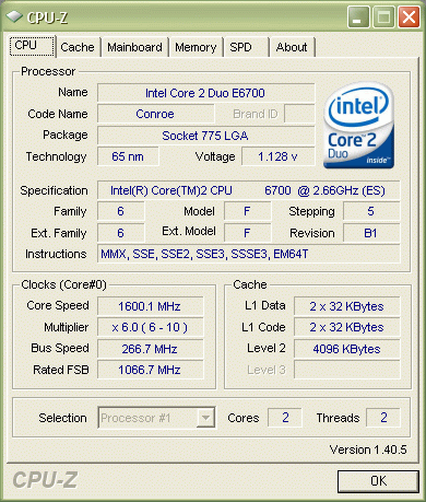 In our test setup, we used the following hardware:
First, let's look as the results of synthetic tests (all the boards are based on Intel X38, except the Blitz version which is based on P35). 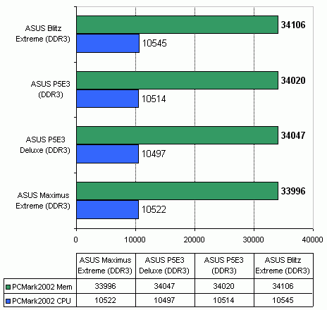 Now on to the gaming benchmarks. 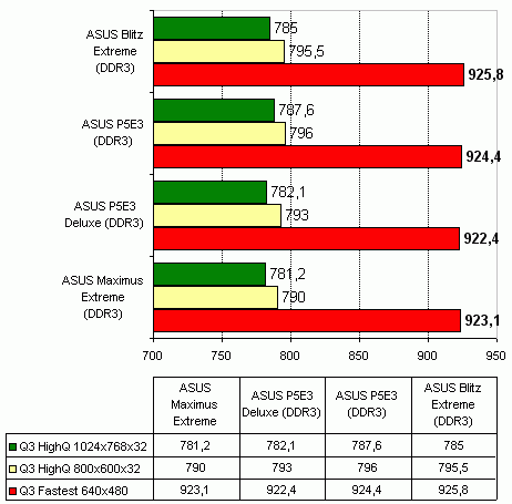 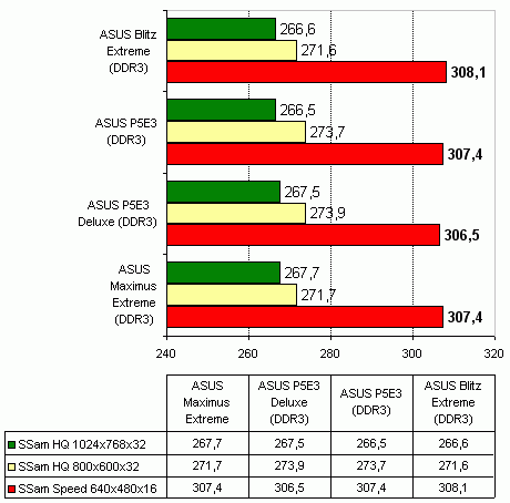 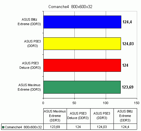 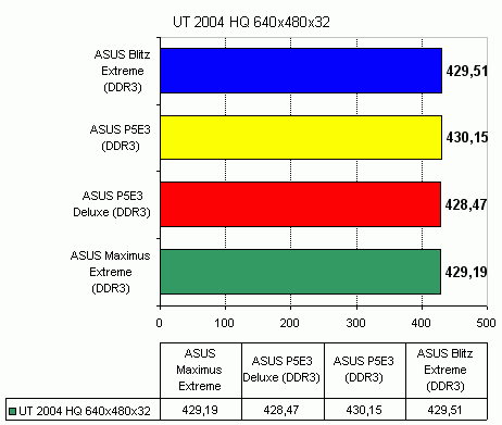 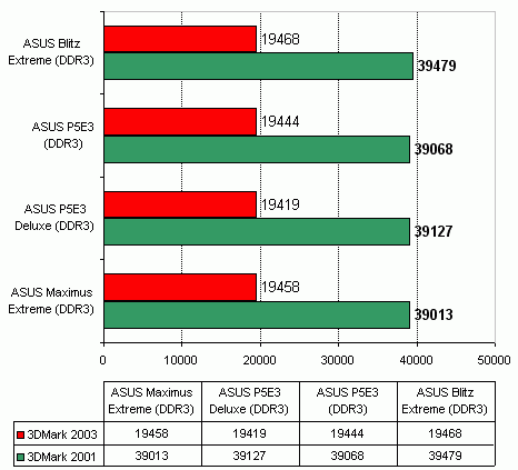 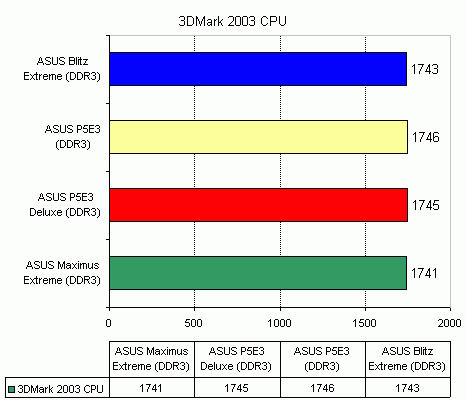 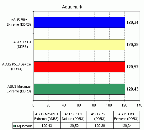 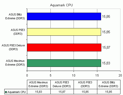 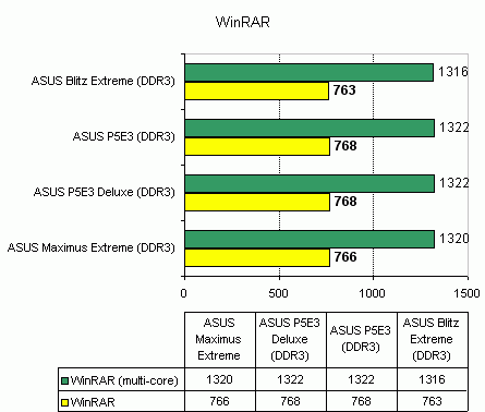 Final WordsFrom the technical viewpoint, we found nothing to complain about both the motherboards. At their specifications, both are outstandingly fantastic products based on the X38 chipset. The expansion options, implementation of proprietary technologies, the workup of the overclocking tools, as well as the design of the integrated cooling system - absolutely all the parts are made at the highest standards. Moreover, both the boards showed record values at overclocking and provided 100% stable clock speed at FSB = 568 MHz. In view of the fact that the Maximus board uses a water block on its north bridge, we can assume that its overclocking capability is even much higher. However, let's not forget that a motherboard is merely one of the mandatory components for a computer. From this viewpoint as well, the attraction of both the products is not so definite. First, both the boards are rather expensive. In particular, as of the late December 2007, there were a few offerings priced at ~$320. The ASUS Maximus Extreme was priced even higher: its price varies within $320 to $380. But that applies to the exclusive Republic of Gamers series, which explains the so overstated price. Certainly, we can choose other motherboards based on X38 of similar specifications albeit at a much lower price. We can give up using the Crossfire technology and then choose a motherboard based on P35, which would be much cheaper. But the problem is not about that! The bottleneck of both the boards is in that they operate with DDR3 memory which costs 8-10 times as much compared to the regular DDR2. Therefore, for the home-based use we don't recommend either ASUS Maximus Extreme or ASUS P5E3 Deluxe. However, we repeat it again, we found nothing to complain about the boards themselves. 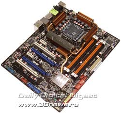 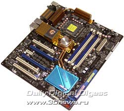
ASUS P5E3 Deluxe vs. ASUS Maximus Extreme
Conclusion
- Discuss the material in the conference
|
|||||||||||||||||||||||||||||||||||||||||||||||||||||||||||||||||||||||||||||||||||||||
|
|||||