NVIDIA GeForce FX5700 Ultra Review
|
NVIDIA FX5700 Ultra
|
| VPU chip |
NVIDIA NV36 |
| Memory |
DDR2 128 Mb; 2.2 ns |
| Frequencies: |
475/950 MHz |
| Category: |
Middle level `2004 |
| Price: |
240$ |
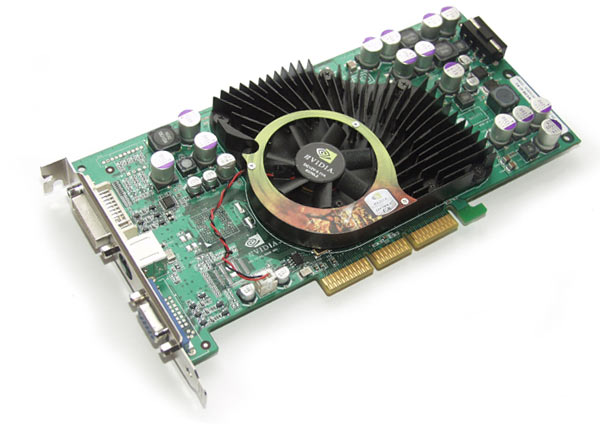
From the very second of examination, the card arouses vague suspicion... Isn't it too "cool" for a mid-end video cards? FX5600 Ultra and Radeon 9600Pro/XT look like tiny dwarfs near it. Its full-sized bulk, huge power stabilizer unit ("My God! The capacitors insides are worth at least 10 bucks!" - exclaimed one of ATI employees when I showed that video card to him), plus a massive radiator - these are just primary exterior attributes of FX5700 Ultra which make it related to Hi-End. The secondary signs are more interesting - the video card offers DDRII (!) 2.2 ns memory onboard, with the 128 MB arranged at 128-bit access.
As our test session "FX5600Ultra vs Radeon9600Pro" last summer showed, NVIDIA practically lost the previous competition round in the mid-end pricing range. This is especially seen from the first revision of the NV31 core. The chip had to be urgently re-made, with the frequencies raised, and the next version already caught up with RV350.
Seems like NVIDIA decided to secure itself against making mistakes.
I. The NV36 (FX5700) chip
Let's start with the NV36 chip that has come take the place of NV31 and win back the crown to NVIDIA in the mid-end pricing range.
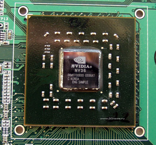
 NV36 / FX5700Ultra Sample (*802x741; 152 kb)
 Version of A1 chip
The chip is made following the 0.13 mk process technology and sports formidable dimensions. On the reference card, there is the "Sample" option which nevertheless didn't prevent it from getting a 120% overclock from its nominal 475MHz to 570 MHz.
And here comes the surprise:
| VGA |
The chip |
Core/
memory speed |
Memory type |
Pixel
pipelines /
Texture units |
Process technology |
Version of
pixel
shaders |
| FX5950 Ultra 256Mb |
NV38 |
475/950 MHz |
256-bit |
8 (4) / 1(2) |
0.13 mk |
2.0 |
| FX5900 Ultra 256Mb |
NV35 |
450/850 MHz |
256-bit |
8 (4) / 1(2) |
0.13 mk |
2.0 |
| FX5700 Ultra 128Mb |
NV36 |
475/900 MHz |
128-bit |
4 (2) / 1(2) |
0.13 mk |
2.0 |
| FX5600 Ultra 128Mb |
NV31 |
~400/800 MHz |
128-bit |
4 (2) / 1 |
0.13 mk |
2.0 |
| FX5200 128Mb |
NV34 |
250/400 MHz |
128-bit |
2 //1 |
0.15 mk |
2,0 |
The very first glance at the tables results in the evident finding - NV36 is in fact NV38 (FX5950) with the number of pixel pipelines halved. That is, both the latest NVIDIA chips - NV38 and NV36 - have been produced on the base of the same core. It's a mystery why no one has yet noticed that :-)
Things with the memory bus are more straightforward - as long as the chip supports 256 bit, it's no problem connecting 128-bit memory to it. That is, the memory bus has been cut-down forcedly. As our tests will show, that was a wise move. The performance of the reference card exceeds all the thinkable limits for today's mid-end video cards and approach the recent high-ends which leaving the rival Radeon 9600XT well behind.
That the chip is unified is quite logical. ATI chose that way a bit earlier. It's too costly to support production and development of three chips at a time for all the pricing ranges. It looks like Hi-end and Mid-end have been merged.
Such approach for the manufacturer suffers from one shortcoming - something has to be done about those overly smart users seeking ways to turn $240 video cards into something worth of a $500 video card :)
Unfortunately, now way.
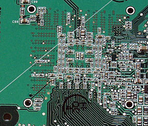
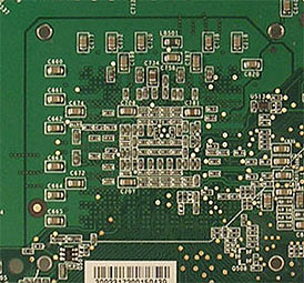
  Unsoldered FX5700 Ultra (left) and FX5950 Ultra (right)
The unsoldering of FX5700 Ultra and FX5950 Ultra differs greatly. As you see, there aren't too many conclusions.
Next 
 |
Content: |
 |
|
- The NV38 Chip
- NVIDIA FX5700 Ultra Video Card Features
- Test configuration. Overclocking
- Benchmarks: Synthetic tests
-
Benchmarks: Gaming benchmarks
 |
Top Stories: |
 |
 |
 |
MoBo:


|
 |
 |
 |
VGA Card:


|
 |
 |
 |
CPU & Memory:

|
|
|

