CPU Intel Core i7-920 (Bloomfield)

Author:
Date: 02.12.2008 |
|
Intel's policies with regard to desktop processors is about renewal of the product line every year. That is done in two ways - migration to a new process technology, and a change of the architecture. Both are quite costly, so every year Intel chooses only one of these. In particular, last year the company migrated to the 45-nm process and presented new products based on the Yorkfield and Wolfdale cores. In 2008, there came a turn for the change of the architecture, and Intel presented its latest development - Nehalem.
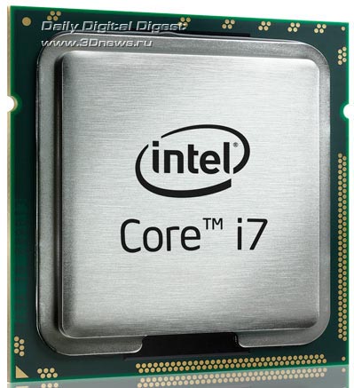
At first glance, we see another revolutionary platform which is able raising the performance bar to another height. We start with the most important, namely, processors based on the Bloomfield core which stand out with the integrated memory controller. As we remember, the first desktop processors with the integrated memory controller were presented by AMD, and that move resulted in a substantial rise of the performance. So we can expect a similar effect from Intel's latest development. However, the integrated memory controller is the most important albeit not the only innovation by Intel. The CPU architecture has acquired a radically new modular structure which features in a new computational core, a new CPU bus, integrated three-channel DDR3 memory controller, integration of the graphic core, the new SMT multi-threading technology, and an additional PCU controller responsible for the control of voltages and frequencies of each of the cores. Needless to say, the new processor architecture called for a change of the CPU socket, so the new processors have the LGA package with 1366 pins.
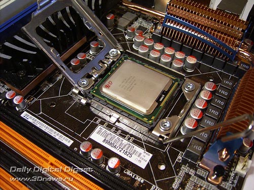
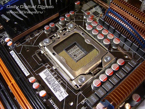
LGA 1366
So, let's examine each of the above items in more detail. First, the new computational core is based on the highly efficient and well-proven Core architecture. Indeed, Core 2 Duo and Core 2 Quad demonstrate a superb combination of high performance, balanced heat emission, and the optimum price. But the Core architecture has some fundamental problems which are not seen to the regular user. The most important of them is the difficulty of scaling or, in simpler terms, in the problems that arise as the number of cores goes up within a single processor. Originally, the Core architecture was developed for use in a two-core make. But once the need for 4-core processors arose, the only possible solution was to merge two dual-core chips within a single package. That resulted in a problem related to the interaction of cores with one another. The thing is, the Quad Pumped Bus has long exhausted its capability and does not allow data exchange among the cores directly. At the same time, its bandwidth did not meet the requirements in multi-core systems. And the more cores, the more vivid the shortcomings of the QPB were. Clearly, Intel could not stand up with that situation and shaped the course towards the increase in the number of cores. That resulted in the birth of the new QPI (Quick Path Interconnects) bus with the "point-to-point" topology. Data is transmitted over two 20-bit wide connections, with 16 bits allocated for data transmission. The resultant bandwidth is 25.6 GB/s, which is approximately equal to that of the HyperTransport v3.0 bus.
The second important change in the architecture of the processor applies to the structure and the size of the cache memory. As compared to the Penryn core, the L1 cache size in Nehalem has not changed. Its size is 64 K, of which 32 K is allocated for data, and 32 K - for instructions. As regards the L2 cache memory size, the changes are more substantial - instead of a large shared cache, the engineers at Intel have equipped each core with its own L2 cache of 256 K in size. Also, Nehalem has acquired the shared L3 cache memory of 8 MB in size (for the Bloomfield core).
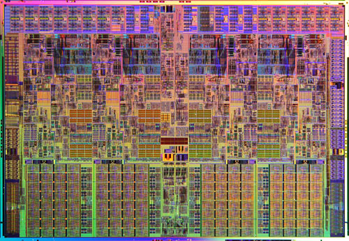
The third and most important change is about the modular structure of the processor, which allows engineers at Intel adjusting the CPU parameters freely enough, through adding specific blocks. In particular, a graphic core and a memory controller can be integrated into the processor. While we can see the integrated graphics not earlier than in 2009, the memory controller is already there in Bloomfield processors. This controller is optimized for operation with DDR3 memory and supports 1-, 2-, and 3-channel access modes. In particular, in using the 3-channel access the bandwidth of DDR3-1066 is 25.6 GB/s, which meets the bandwidth of the QPI bus. Therefore, for the Socket LGA 1366 platform the faster memory is not yet needed for now.
3-channel mode
We also note that on motherboards based on the X58 chipset there will be at least three DIMM slots for DDR3, and the standard number of slots will equal 6:
6 DDR3 slots on ASUS P6T Deluxe motherboard
Apart from the listed traits of the Nehalem architecture, it makes sense to mention some minor modifications of the computational core itself. The engineers at Intel took the kernel of the Core architecture and modified some of the functional blocks like decoders of simple (3) and complex (1) commands, improved the Macrofusion technology (x32/x64) (execution of a number of commands (up to five) as a unified instruction), optimized the Loop Stream Detector, the Stack Buffer, increased the capacity of the Reorder Buffer / Reservation Station aimed ay the SMT technology. By the way, the latter technology deserves to be examined in more details.
In using the Netburst architecture, the engineers at Intel were working hard at the load optimization and execution of commands in rather long pipelines (a distinctive feature of this architecture). Of the technical solutions for this problem was the HyperThreading technology which allows for a simultaneous execution of two command streams at a time by a single CPU core. In the end, the user could see the doubled number of CPUs in the system, and that technology gave some performance gain in optimized applications. On the other hand, in non-optimized applications (e.g., games) the user came up against the situation when the system with the HyperThreading enabled was working somehow slower. In the new Nehalem architecture, engineers at Intel tried to eliminate all the bottlenecks of the HyperThreading, and the final result was given the name Simultaneous MultiThreading (or SMT). One of the traits of this technology is division of the cores into real and virtual, which allows for their more efficient use (from the software developer's viewpoint).
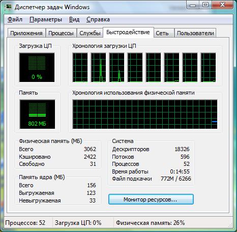
4 real cores + 4 virtual cores
A few words on the physical parameters of the new Nehalem core. The first Core i7 CPUs offer the core area 263 sq. mm, and the core itself is made up of 731 mln transistors. At the same time, the typical heat emission level remains within Intel's specifications and amounts to 130W. This indicator can be regarded as quite acceptable in view of the increased complexity of the core. By the way, one of the leading roles in the power-saving is played by the Power Control Unit responsible for the current clock speed and voltages of each of the cores depending on the load. Moreover, the PCU can disable inactive cores completely.
Interestingly, the PCU is quite closely linked to the Turbo Boost technology which also controls the frequencies of the cores, but it is aimed at raising the frequency. The frequency is adjustable through variation of the multiplier, so the multiplier has to be unlocked towards the increase. This is just what engineers at Intel did, albeit with some reservation: the multiplier can be increased by only 1 from the nominal. In practice, this looks like this:
The multiplier higher that the standard by 1
Now let's make up the interim totals and compare the parameters of the Bloomfield and Yorkfield cores.
| Core |
Bloomfield |
Yorkfield |
| Process Technology |
45 nm |
45 nm |
| Cores/chips |
4/1 |
4/2 |
| Support for multithreading |
SMT |
- |
| Integrated memory controller |
3-channel DDR3 |
- |
| L1 cache |
64 K (32+32) |
64 K (32+32) |
| L2 cache |
4x 256 K |
2x 6 MB |
| L3 cache |
8 Mb |
- |
| Bus type/frequency |
QPI / 133 MHz |
QPB/ 266, 333, 400 MHz |
| TDP |
130 W |
130 W |
| Packaging |
LGA 1366 |
LGA 775 |
| Support for SSE |
SSE 4.1, SSE 4.2 |
SSE 4.1 |
| Core area, (sq. mm) |
263 |
2x 10⁷ |
| Transistors (mln) |
731 |
2x 410 |
| Power supply/frequency control |
Speed Step; PCU + Turbo |
Speed Step; |
We have sorted it out with the Nehalem architecture. Now let's look at the assortment of first processors based on the Bloomfield core:
| Name |
Core i7 965 Extreme Edition |
Core i7 940 |
Core i7 920 |
| Q-ty of cores |
4 |
4 |
4 |
| Support for SMT |
+ |
+ |
+ |
| Clock speed |
3.20 GHz |
2.93 GHz |
2.66 GHz |
| Multiplier |
24 |
22 |
20 |
| QPI bus |
6.4 GT/s |
4.8 GT/s |
4.8 GT/s |
| Supported memory |
DDR3 -800/1066/1333/1600 |
DDR3-800/1066 |
DDR3-800/1066 |
| TDP, W |
130 |
130 |
130 |
| Recommended price, $ |
999 |
562 |
284 |
We've got the weakest processor of the new line - Core i7 920. Because of the increased number of pins, its dimensions are somehow larger than those for LGA775:
To the left - Bloomfield, to the right - Conroe
The CPU-Z utility displays the following information:
 |
Content: |
 |
|
 |
Top Stories: |
 |
 |
 |
MoBo:


|
 |
 |
 |
VGA Card:


|
 |
 |
 |
CPU & Memory:

|
|
|
